
An exceptional electronic product is more than just an optimised circuit layout; it must be protected, powered, and housed within a robust physical chassis. Designing an enclosure for a Printed Circuit Board Assembly (PCBA) requires a delicate balance between electrical functionality, mechanical durability, and manufacturing constraints.
Whether you are modifying an off-the-shelf stock housing or engineering a highly complex, custom injection-moulded enclosure, synchronisation between electrical and mechanical engineering disciplines is critical to avoiding fitment failures and delayed product rollouts.
The Paradigm Shift: Concurrent ECAD-MCAD Design
Historically, the design process followed a linear path: an electrical engineer finalised the PCBA layout, exported a 2D drawing, and handed it to a mechanical engineer to build an enclosure around it. This siloed approach frequently led to hidden interference points, misaligned connectors, and poor thermal airflow.
Modern electronics engineering relies on concurrent engineering via a unified digital twin. Mechanical step files of the enclosure housing, structural mounting standoffs, and screw bosses are imported directly into the ECAD (Electronic Computer-Aided Design) environment at the very start of the layout phase. By utilising real-time bidirectional data exchange formats like IDX or universal STEP files, engineers can position component footprints, align input/output ports (like USB-C, RJ45, or barrel jacks), and verify critical Z-axis component heights dynamically.
Primary Architectural Paths: Stock vs. Custom Enclosures
Depending on your production volume, time-to-market constraints, and target manufacturing cost, your project will dictate one of two structural enclosure routes:
1. Custom Enclosure Engineering (Injection Moulding & 3D Printing)
- Best For: High-volume commercial products, tight space constraints, and unique brand aesthetics.
- Design Consideration: Demands rigorous attention to DFM (Design for Manufacturing) rules, including uniform wall thicknesses to prevent plastic sink marks, draft angles for mould release tool pathing, and expensive upfront tooling costs. For rapid benchmarking and physical integration verification, additive prototyping methods like Stereolithography (SLA) or Selective Laser Sintering (SLS) are deployed before cutting steel tooling moulds.
2. Modifying Off-the-Shelf Stock Enclosures
- Best For: Low-to-medium production volumes, rapid prototyping, and cost-conscious industrial hardware.
- Design Consideration: Leading global component suppliers hold inventory for thousands of pre-moulded plastic and extruded aluminium enclosures, providing precise mechanical DXF drawings. These housings are customised by CNC machining precise cutouts for connectors, display apertures, and indicator LEDs. This path completely avoids expensive injection mould tooling overhead.
5 Critical Engineering Factors for Enclosure Integration
When designing a chassis, you must account for several mechanical and physical environmental constraints to ensure the survival of the enclosed electronics.
1. Mechanical Clearances and Interferences
Always implement a tolerance stackup analysis to compensate for variations in manufacturing.
- X/Y Board Tolerance: Leave a minimum perimeter gap of 0.5mm to 1.0mm between the edge of the PCB and the internal wall of the enclosure to account for routed edge deviations during board depanelisation.
- Z-Axis (Component Height) Clearance: Account for the height profile of the tallest components (such as large electrolytic capacitors, inductor coils, and transformers) with a buffer of at least 1.5mm to 2.0mm below the internal top surface of the enclosure wall.
- Connector Protrusion: Surface-mount or through-hole connectors extending through enclosure walls should project out by 1.0mm to 1.5mm beyond the chassis exterior to ensure secure cable mating connections.
2. PCB Mounting Options and Structural Integrity
Securing the PCBA inside the enclosure protects fragile solder joints from flexure and vibration stress.
- Method A: Threaded Standoffs and Screws
The board rests on structural bosses moulded directly into the housing. Plastic thread-forming screws or metal brass inserts (heat staked into place) securely clamp the PCB via dedicated mounting holes. Ensure that no component traces or ground plane copper rings encroach on the physical screw head clearance zone (the “keep-out area”).
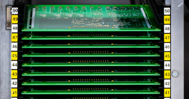
- Method B: Slide-In Card Guide Slots
Extruded aluminium or moulded plastic enclosures often feature integrated internal tracks or vertical slots. The parallel edges of the PCB are slid down into these guides, eliminating the need for mounting hardware. This approach requires your layout engineer to maintain clean component keep-out regions directly along the physical edges of the board.
- Method C: Snap-Fit Retention Clips
The PCBA is pressed over flexible moulded plastic hooks that deflect outward and snap over the top face of the board. Ideal for fast, toolless assembly lines, this method requires tight mechanical tolerances to prevent excessive board flexing during production assembly.
3. Thermal Management and Convection Airflow
Enclosures trap heat generated by power conversion ICs, high-speed microprocessors, and voltage regulators. Without passive or active mitigation strategies, thermal accumulation will shorten component lifespans:
- Passive Convection: Position ventilation louvres or perforated slots at both the base and top of the enclosure to induce a natural chimney effect, pulling cool ambient air across the board.
- Conductive Heat Sinking: For sealed, weatherised enclosures where air vents are not permitted, use silicone thermal gap pads to bridge high-power components directly to an aluminium chassis body or an internal heat sink, transforming the outer enclosure surface into a radiator.
4. Environmental Ingress Protection (IP Ratings)
If your electronic device will operate in harsh environments exposed to rain, dust, or chemical oils, your enclosure must be engineered to a target Ingress Protection (IP) code.
- Sealing Gaskets: Incorporate precision elastomeric or silicone O-rings along the split mating seams of the enclosure halves.
- Fastener Isolation: Ensure that exterior assembly screw holes are located outside the perimeter sealing gasket path or sealed independently with specialised compression washers.
5. Electromagnetic Interference (EMI) Shielding
Non-conductive plastic enclosures provide zero protection against electromagnetic fields, running the risk of failing emissions compliance certifications (like FCC or CE).
- Conductive Coatings: For plastic enclosures, apply an internal layer of conductive copper or nickel-loaded EMI shielding paint.
- Metallic Enclosures: Utilising extruded or die-cast aluminium enclosures provides an inherent Faraday cage, provided the internal ground plane of the PCBA makes a direct, low-impedance electrical contact to the metal chassis via an unmasked mounting hole.
Seamless Handoff to Production
To achieve a professional, commercial-grade fit on small or large manufacturing runs, the production files for your PCBA and enclosure must be cross-verified.
When configuring your engineering package for a full-turnkey build at PCB Train, our CAM team cross-references your electronic Gerber/ODB++ layout data with your mechanical enclosure files. This unified approach guarantees that components, milling pathways, and mounting hardware match perfectly, giving you a functional and high-yielding final assembly.
Get a quick online quote today.
Original article written: November 2013. Updated: June 2026
Philip King
Latest posts by Philip King (see all)
- How to Design an Enclosure for a Printed Circuit Board Assembly (PCBA) - 18th June 2026
- Understanding IPC Standards in PCB Fabrication and Assembly - 2nd June 2026
- SMD PCBs: What They Are And Where They Are Used - 7th October 2022


Leave a Reply