





The evolution of modern electronics can be traced through a single, defining transition: the shift away from bulky wires towards compact, automated assembly. At the heart of this revolution is Surface Mount Technology (SMT), the PCB manufacturing process responsible for almost every compact electronic device in existence.
SMT vs. Through-Hole Technology (THT)
Before SMT achieved dominance, circuits relied entirely on through-hole technology (THT). Still used today, THT requires component leads to pass completely through drilled holes in the circuit board, where they are soldered on the opposite side. While THT remains useful for high-stress connectors and heavy power components due to its superior mechanical strength, SMT takes a completely different approach.
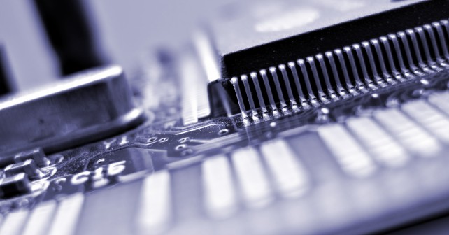
With SMT, components, known as SMDs (Surface Mount Devices), are soldered directly onto flat copper pads on the board’s surface. By removing the need for millions of drilled holes, SMT allows components to be placed much closer together, enables dual-sided population, and massively reduces the overall footprint of the device.
The SMT Assembly Process Step-by-Step
Modern SMT assembly lines are marvels of high-speed automation. The process is broken down into four critical phases:
Phase 1: Solder Paste Printing
A precision metal stencil is aligned over the bare PCB. A squeegee blade sweeps across, depositing a precise volume of solder paste onto the surface pads. For highly complex or prototype boards, advanced jet printers apply solder paste dots directly without needing a physical stencil.
Phase 2: Automated Pick-and-Place
High-speed robotic heads fitted with optical alignment cameras and vacuum nozzles pull SMDs from component reels. These machines place components onto the sticky solder paste at speeds exceeding tens of thousands of parts per hour, handling packages as minuscule as the 0201 or 008004 standards.
Phase 3: Reflow Soldering Oven
The populated board travels on a conveyor belt through a multi-zone reflow oven. The oven carefully ramps up the temperature to activate the flux, liquefies the solder alloy (typically reaching peak temperatures of 240–250°C for lead-free SAC305), and then cools to form durable, metallurgical joints.
Phase 4: Automated Inspection
The completed assembly passes into an AOI (Automated Optical Inspection) system. High-resolution cameras and multi-angled lighting check for component misalignments, tombstoning (components lifting on one end), or solder bridges. For hidden connections like BGAs (Ball Grid Arrays), 3D X-ray systems are used to verify internal joint structure.
The Engineering Benefits of SMT
- Component Miniaturisation: Allows microcontrollers and passives to scale down to fractions of a millimetre.
- Enhanced Electrical Performance: Shorter paths mean reduced parasitic inductance and capacitance, vital for high-frequency RF and high-speed data circuits.
- Cost Efficiency: Highly automated assembly drops manual labour costs to near zero for volume production runs.
At PCB Train, our large-scale UK assembly facilities leverage modern pick-and-place precision and reflow profiling, allowing us to build everything from ultra-dense prototypes to ongoing production runs with exceptional yield rates. Get in touch today for a quick quote.
Updated: June 2026.

Philip King
Latest posts by Philip King (see all)
- How to Design an Enclosure for a Printed Circuit Board Assembly (PCBA) - 18th June 2026
- Understanding IPC Standards in PCB Fabrication and Assembly - 2nd June 2026
- SMD PCBs: What They Are And Where They Are Used - 7th October 2022


Leave a Reply