
What to consider when designing and laying out a PCB
To prevent lost time or costs later on down the line, you must be careful with your PCB design and layout. Function and reliability problems can easily be caused at early stages and throw off your entire project/device. This piece is designed to help you make your projects work as you intend them to.
PCB based devices, at their core are designed to solve a problem. Electronic systems generate voltage waveforms. These waveforms contain information that is then used by circuits to perform a task. The idea behind creating a device involves using waveforms to successfully perform the task without interference from noise or signals. Understanding the basics helps – but you need more to ensure the success of a circuit. PCB design mistakes can cause many headaches down the road.
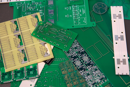
Almost every single electronic device is made up of printed circuit boards. Many different elements need to be considered when designing a PCB – especially when performance is a key factor. Common issues around PCBs include your design expectations, via types and capacitance. The importance of these three issues is magnified when designing high speed or complex PCBs. This will be a beginner guide to some of the more common issues.
Making a design that works – ensuring your expectations are in check
Printed circuit boards are composed out of many different parts and devices. A common theme is that these parts are not perfect. There are delays from inputs to outputs even among the exact same end product. Time delays exist from each end of a wire or transmission line. Power distribution systems innately have defects which compromise performance. Capacitors have parasitic capacitance, which will be discussed more later on. These issues allow for the complexity of circuit design. These margins for error need to be minimised as much as possible to produce a design that functions entirely as expected. Understanding what causes these changes means there will be less possibility for errors overall. Keep all of this in mind in the initial stages of your design.
Sizing for copper traces
Copper traces have different levels of resistance depending on the result of resistivity times length divided by the result of thickness times width. The best way to change this as a designed is to look at adjusting trace size, as other aspects are not controllable. You can do this by changing the length, thickness and width.
Size for loops
All loops on your board should be as small as possible. This keeps your inductance and resistance low. This reduces noise or high frequency voltage spikes that can occur.
Seperate digital and noisy traces from analog traces
Noisy and high frequency traces must be kept seperate from analog traces. Keeping them close together can group their signals together.
Bill of materials
This is essential to be generated early on in the process. The components in the circuit should be chosen based on an analysis of operating voltages, tolerance and electrically satisfactory components. Less technical elements also have to be considered like availability, budget and size. Be sure when creating your bill of materials to be aware of how your manufacturer treats components. PCB Train for example hold over 1000 different parts that are completely free. Keep in mind that hard to source parts can be expensive or time consuming and may also delay assembly. Specify components in your BOM by stating the manufacturer’s name and part number.
Via types
Vias provide electrical access from one layer to another – they’re holes drilled into the PCB. They can either change from one layer to the next – or be used as component pins using through hole or surface mount techniques. The relevant holes are then plated with copper to provide the necessary connection. On a basic level – there are three types of vias: through hole vias, blind vias and buried vias.
Through hole vias
The most common via type are through hole vias. They’re often created with mechanical drills followed by electroplating. The ratio of length to diameter needs to be considered for this kind of via. This is also known as aspect ratio. High volume manufacture should have an aspect ratio of below 6:1. High performance PCBs can be extended to 8:1 if necessary. 10:1 is an absolute limit and requires special process control.
Blind vias
Vias that are located on one side of a PCB but don’t pass all the way through to the other side, are known as blind vias. They can also be known as a microvia – this is defined as a via with a diameter less than 8 mils regardless of whether it passes through the PCB. There are four main ways to create a blind via. Control depth drilling, laser drilling, sequential lamination and photo imaging. When a very accurate drill machine is programmed to drill only part way through the PCB – it is known as controlled depth drilling. This method of course relies on the area below the via being free of conductors to give a tolerance for drill overshoot. Laser drilling involves the use of a high power laser beam to drill through the copper, and then the first layer of the dielectric. It then stops at the copper pad which serves as the connection to the second layer down. This then needs a pad to be used to stop the laser beam. The beam needs to be strong enough to remove all of the resin and glass – but not enough to remove the inner layer pad. This makes this technique fairly complex. Photo imaged vias take shape by applying a mask-like photosensitive material. Panels need to have gone through the normal lamination process for the inside n-1 layers including the traces being etched on it. It’s then exposed and developed to create openings that form the blind vias. The holes are then opened with CO2 laser (which will not cut through copper) down to the buried layer. The outer layer then has copped plated onto it to make contact to the inner layer pad. This is a complex process but can be used to form blind vias on PCBs in volume. Most HDI laser drilled circuits are drilled using CO2 lasers.
The use of UV lasers
However, for lower volume PCB manufacture, UV lasers are suitable. UV lasers are slower to drill holes than CO2 lasers, but will cut both copper, glass and resin by ablation, and the depth of cut is highly controllable by managing the point of focus of the beam. This method is only suitable for holes up to around 200 microns diameter and 200 microns deep, so is very suitable for microvias.
Sequential blind vias
Sequential blind vias are created by forming a two-sided PCB from just the first and second layer. This thin piece of laminate is drilled, plated and etched as if a two layer were being made. It’s then combined with all of the other inner layers. It’s then laminated, drilled and plated just like it would be for any multilayer PCB. This is a delicate and expensive process however.
Buried vias
Buried vias are located between a minimum of two inner layers without reaching the surface of any layer. The process for these is very similar to sequential blind vias. PCBs with buried vias cost more as a result. Be aware that these vias are not often used in commercial applications due to the high cost.
Capacitance
Printed circuit boards may well be familiar to you – their layout is essential in the correct functioning of circuitry. There are many different aspects to consider, for newcomers and those who are feeling a bit rusty on the subject. Key to the performance of a circuit is capacitance. We want to empower you with this article by showing you the how’s and why’s so that you can understand it enough to make your own decisions. Often parasites or parasitic can harm your circuit – this is especially true for high speed circuits. In these instances, changes can cause instability and oscillations more easily. Usual causes involve poor spacing between power and signal traces. The extent to which they need to be considered however does depend on the individual circuit.
What is capacitance and why is it important?
Capacitance is defined as the property of a collection of conductive structures that causes electrical charge to be stored on them when there’s a voltage difference between them. Named after an early researcher into electromagnetic effects Michael Faraday – a basic unit of capacitance is a Farad. It’s defined as the capacitance of a capacitor where a charge of one coulomb produces a one-volt potential difference between its terminals. The capacitance that exists between transmission lines or wires and the surrounding structures (likely to be the planes for a PCB) must be charged up in order to change the voltage on the transmission line from a logic zero to a logic one. An electromagnetic wave does this. This “parasitic” capacitance then impedes the changing of the signal voltage of a transmission line. The charge that is then deposited onto signal lines to change their logic states or voltages is actually the main consumption of power in switching circuits.
It’s worth noting that over time the current flow actually raises the voltage across the capacitor. The current flow over time or charge that’s required to raise its terminal voltage is also higher if the capacitor is larger. If the parasitic capacitance of a circuit is large, it’ll take more power to perform a given logic operation. The main way to increase the speed of logic circuits for a given power consumption has been to reduce the parasitic capacitance of each element of the circuit. Increasingly smaller IC transistors and wires have made this possible.
The relative capacitance of parasitic elements that exist on real transmission lines may be measured in pico-farads or nano-farads. The place where this has the most effect is on transmission lines that have to be charged and discharged in order to change logic states. Sine waves can be impressed across capacitors to exhibit impedance to the low of current through it so it can be calculated.
Be wary of parasites
Impedance of parasitic elements is dependent on the frequency. At low frequencies, any parasitic capacitance that exists in the part of an electromagnetic field has no detectable effect and can be ignored. As a result they have little to no effect on performance as long as the frequency is low. As frequencies approach a GHz, parasitic capacitance from structures such as plated through holes, oscilloscope probes and the input capacitance of each load can have a noticeable effect on signal quality. Parasitic capacitance elements that normally occur in signal paths have detectably low impedance and can have an adverse effect on signals.
Capacitance best practice
Capacitance can be used in beneficial ways however. Two of these ways are as charge storage devices, usually known as decoupling capacitors or bypass capacitors. Couple capacitors can also be used to pass an AC signal while blocking a DC signal. Another beneficial use of capacitance is as part of a switching power supply in the form of storing charge when converting one DC voltage to another. When the reactance of the capacitor is exactly equal to the reactance of the inductor,this is known as impedance low. When the frequency Fr (self-resonant frequency of the network) is reached, the two reactive components cancel each other out. Beyond that frequency, the impedance goes back up. This is due to the parasitic inductance – this makes the capacitor behave more like an inductor than a capacitor. This can have negative effects in regards to the functioning of the circuit.
Choosing a PCB supplier
An essential part of this process revolves around choosing a PCB supplier or fabricator that is capable of supplying prototype and production quantity PCBs of the type used in your PCB. Fabrication is an immensely complicated process and requires a high level of skill. An important part of the process is looking at the whole picture. First time customers often choose based on the price of the PCB. Other areas that have to be considered are test, repair, replacement (if necessary) and miscellaneous other costs. Fabricators have to be chosen with the thought of keeping failed prototypes and production PCBs to the minimum. Be sure to view testing policies as well as everything you can about the company you choose. Luckily, once you’ve found a good one you can rest safe in the knowledge that you can use them again.
If you found this helpful then please let us know! If you have any questions regarding this or other topics then feel free to comment and we’ll cover it in the future.
pcbtrain
Latest posts by pcbtrain (see all)
- Rapid PCB Prototyping with PCB Train Express - 5th July 2023
- 5 Good Reasons Why You Should Use PCB CAD Layout Design Services - 14th June 2023
- How To Become A PCB Designer - 1st November 2022


Leave a Reply