
CLICK TO START YOUR ORDER:


Single layer vs multi layer PCBs
When it comes to printed circuit boards, an immediate question before design is whether to use single or multi layered PCBs for your circuit. The benefit and use of each depends entirely on what you’re intending to do. First, we should define each type of circuit board.
Single layer or single sided PCBs
These PCBs simply have components on one side of the board and the conductor pattern on the other side. This reason is why it’s known as a single sided or single layer PCB. Often, these are used for simpler devices as no wires can cross if the circuit is to function correctly. These are usually slightly cheaper to manufacture than multi layer PCBs.
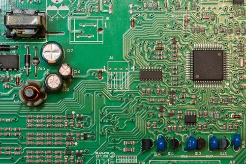
Multi layer PCBs
Multilayer PCBs have one or multiple conductor patterns inside the board, this increases the area available for wiring. By laminating or gluing several double-sided circuit boards together with insulating layers in between. Frequently, between 4 and 8 layer PCBs are used as these offer the right amount of complexity for most purposes. There is the capacity for more layers however depending on device. These are likely to be different depending on the various device. Some smart phones for example are said to use 12 layers due to the various demands of the circuit. Often they have an even number of layers as odd layers can lead to issues with the circuit board. This includes problems like warping and twisting after soldering, and no cost savings as they’re not the standard to produce.
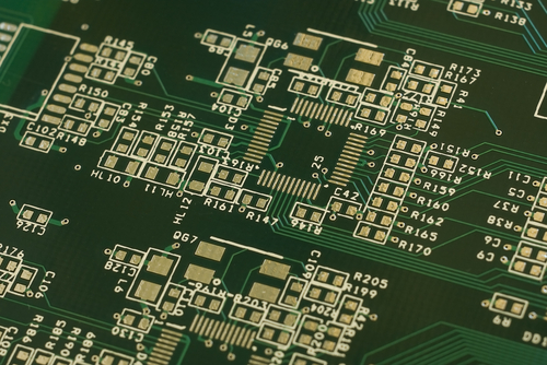
How to identify a multi layer PCB
If you have some PCBs to hand and you’re interested in how many layers it uses, there is a way to see without causing damage to the board itself. Helpful suggestions from a user called “Nick T” from stackexchange suggest the following:
- Firstly, shine a light into the edge in an attempt to see the copper planes, this may result in you seeing the signal traces. This will only work if the copper comes close to the edge however.
- Using some sort of bright light source again, we can see if a board has inner layers even if doesn’t have blind vias. The best place to do this is “where there aren’t traces/planes on the visible, outer layers…” The areas where it’s blocked are usually copper.
- Some companies or manufacturers are known to label the individual layers on the board itself, so check around the edges for numbers.
Common uses for multi layer PCBs
- Computers
- Mobile phones
- Heart monitors
- X ray equipment
- GPS technology
Downsides of multi layer PCBs
There are some cons to the multi layer PCB, so be sure to keep the below in mind when using a multi layer PCB:
- Higher manufacturing costs
- Potentially longer manufacturing time
- More complex repairs
Who’s the winner for you?
We hope that you have found this information useful. If you have any questions then please ask and we’ll get back to you. At PCB Train, we manufacture 2 layer, 4 layer multi layer and 6 layer multi layer PCBs, with further configurations completed by our sister company, Newbury Electronics. We also have an online quote and price calculator to help you make the most informed decision possible. We manufacture single sided, single layer and multi layer PCBs with fast lead times and competitive pricing.
Philip King
Latest posts by Philip King (see all)
- How to Design an Enclosure for a Printed Circuit Board Assembly (PCBA) - 18th June 2026
- Understanding IPC Standards in PCB Fabrication and Assembly - 2nd June 2026
- SMD PCBs: What They Are And Where They Are Used - 7th October 2022


Leave a Reply