
CLICK TO START YOUR ORDER:
The Basic Set Up of a PCB
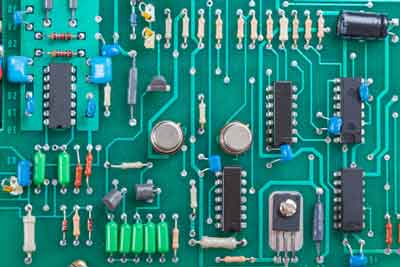
As you probably know, printed circuit boards are pretty ubiquitous in the world of electronics. You will probably find one in the devices that you use every day. However, people often use these electronic devices without considering or understanding the technology behind them. Here are the basics of PCB design, components and construction to give you a better idea of how your electronics operate.
In its simplest form, a PCB is a plastic board reinforced with glass. Attached to this board are copper lines and pads which connect together, cut from a copper layer. These copper lines (known as traces) allow electrical charge to flow through the PCB, providing power to the different components that are situated systematically on the board. The copper traces function in the place of wires, guiding the electricity to the correct destination.
The Layers of a PCB
The simplest PCBs are single sided boards (one copper layer). However, the copper traces can also be installed on both sides of the board, creating a double sided PCB. They become more and more complex as additional layers are added to the original design. These new layers have their own copper trace formations. The copper connections cannot cross one another without the path of the electrical charge being compromised, so multi layered PCBs become necessary for advanced electronics. However, in the single sided boards one side is reserved for the copper trace and the other side houses the components.
On top of the copper layer sits the solder mask and the silkscreen. The solder mask is what makes the PCB its recognisable green colour. This has the function of insulating the copper from any metal parts that might accidentally come into contact with it. However, parts of the metal will remain exposed so that they can be soldered to. The silkscreen sits on top of the solder mask again. This has letters and numbers drawn on it which makes the assembly of the PCB easier for the engineer (or the hobbyist!).
PCB Components
If the copper traces behave like the skeleton of the PCB, acting as its basic structure – then the components are the vital organs. Each one has a different function. They give the circuit the unique qualities that make it fit for its intended purpose. Depending on the device or electronic item a PCB is designed for, different circuit board components will be needed for different circuits. These components can consist of a wide range of electronic parts. Some common PCB components include:
Battery: provides the voltage to the circuit.
Resistors: control the electric current as it passes through them. They’re colour coded to determine their value.
LEDs: light emitting diode. Lights up when current flows through it, and will only allow current to flow in one direction.
Transistor: amplifies charge.
Capacitators: these are components that can harbour electrical charge.
Inductor: stores charge and stops and change in current.
Diode: allows current to pass in one direction only, blocking the other.
Switches: can either allow current or block depending if they are closed or open.
PCB Assembly
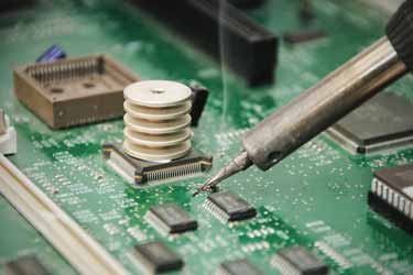
These components can be attached to the board in various ways. In general, an engineer will choose to use either the surface mount method or the through-hole method to attach the components. Following a schematic pattern and using the numbers on the silkscreen, the engineer uses solder to attach the components to the board. The engineer must be very careful when soldering. As solder is a metal that an engineer melts so that they can manipulate it. Any stray blobs that are out of place and touch other metal components could cause the circuit to short. This can be dangerous, causing fires or even small explosions. When the components are installed correctly, the PCB is ready to be used in a device.
So, there you have it. The basic design, construction and components of a PCB. This is only an overview, as PCBs can get extremely complex with advanced electronics. However, the basic principles remain the same, even with 16 layered boards.
If you’re considering PCB assembly, manufacture, fabrication, solder paste stencils or any other PCB production – get an online quote now.
Philip King
Latest posts by Philip King (see all)
- How to Design an Enclosure for a Printed Circuit Board Assembly (PCBA) - 18th June 2026
- Understanding IPC Standards in PCB Fabrication and Assembly - 2nd June 2026
- SMD PCBs: What They Are And Where They Are Used - 7th October 2022


test