
1. Why they’re green
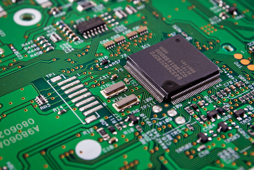
Have you ever wondered why the majority of PCBs are that iconic dark green colour? The green that you see is actually the colour of the soldermask showing through the glass. In regards to the origins of the use of the green, there are a few theories.
Some speculate that green was the regulation standard when for when PCBs were used by the American military, and the use of it spread from there. It has also been suggested that green could have been the colour of the original solder mask resins, and that we continue to use green as a matter of convention, despite no longer using these materials. In modern circuits a soldermask can actually be made in any colour. However, green has worked well for us so far, and it makes it particularly easy for engineers to see faults in the traces, so many companies tend to stick with it.
2. Who invented them?
The invention of the PCB is generally accredited to Paul Eisler, an Austrian inventor, though the development leading up to the invention can be traced back to the 1890s. Eisler developed the first PCB when working on a radio set in 1936. However, PCBs didn’t see mass usage until after the 1950s, and their popularity grew hugely from there.
3. They are everywhere!
You might not have considered just how ubiquitous printed circuit boards are. You’re probably within touching distance of a device that makes use of one right now. You’re likely reading this from a device that contains a PCB! They’ve become a really integral aspect of modern tech, and as PCB technology itself is constantly evolving, it doesn’t look like any other creations will be replacing them any time soon.
4. They’re designed using CAD
You might not know that PCBs are designed using CAD, or computer aided design. Technicians use CAD programs to design both the schematic and the layout of the PCB. This allows the board design to be tested, checking that all the traces are properly connected before the PCBs are physically made.
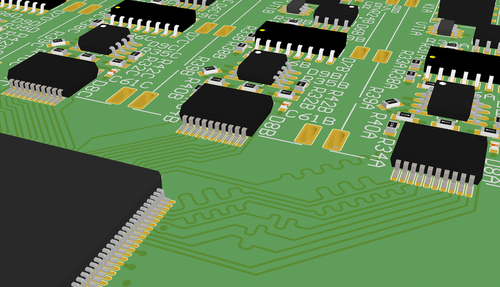
5. Surface mount technology
Surface mount technology (or SMT) is the most common manufacturing technique used to make modern PCBs. SMT became widely used in the 1980s and quickly replaced its predecessor, the through-hole method, which had been slow and incurred many errors. Whereas with through-hole the components had to be attached to the board by inserting component ‘leads’ into holes, SMT sees them glued onto pads on the PCB’s surface.
6. Traces not wires
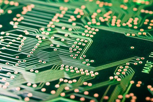
You probably know that electronic devices most commonly use wires as a means of transmitting energy. However, PCBs are an exception to this convention. Instead of wires, PCBs use copper traces to transport electrons. Using copper traces in the place of wires allows PCBs to be a lot smaller, as the flat traces take up a lot less space. It also means that they can be made using through-hole technology, as the copper can easily transfer through a hole in the circuit board.
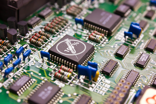
7. There are lots of potential components
There are probably more components used in PCBs than you’ve ever imagined, and they all have their own individual properties. The list includes (but is not limited to); resistors, potentiometers, capacitors, inductors, relays, batteries, fuses, transformers, diodes and transistors. A list of what the main PCB components are and their functions can be found in our previous blog about PCB design, components and construction.
8. Silkscreens
Have you ever wondered about the white etchings that you seen on top of the green PCB soldermask? This is the silkscreen, and it is used on the component side of the circuit board to identify components and other PCB information. The white text can be silk screen printed, which is where it gets its name, but it is increasingly printed using digital by ink-jet printers.
9. They can be completely personalised
Companies like PCB Train make circuit boards entirely to order. You can order them to suit whatever specifications you need. But there is no need to make every PCB to a unique specification. Custom PCBs will be expensive. The good news is that 99% of all PCBs bought can be specified within the parameters of 14 standard services available from PCB Train. Because they are standardised specifications, manufacturing costs are significantly lower.
10. The technology is always changing
PCBs have changed hugely since the days of Paul Eisler in 1936. They’re so much smaller, faster, and more efficient to build. However PCB technology is always evolving. Right now scientists are working on making PCBs that are biodegradable. Similarly, the development of the material ‘graphene’ could change the ways in which our electronics operate. PCBs are never static; the technology is always developing.
11. They’re getting smaller
 The pressure on developers to make smaller and smaller electronics has had an impact on PCBs – they’ve had to become smaller too! Surface mount designed PCBs are up to one tenth of the size of through-hole circuits. This miniaturisation is set to continue, as detailed in this blog from Newbury Electronics.
12. They’re subject to laws (Ohm’s Law)
The rules of physics strictly govern over printed circuit boards. The most famous of these amongst electrical engineers is Ohm’s Law. Ohm’s Law dictates the relationship between current, resistance and voltage. Stated simply, it is the principle that electrical current is proportional to voltage and inversely proportional to resistance. These laws dictate the ways in which we can design and build our PCBs, so an electrical engineer has to have a full understanding of their implications.
pcbtrain
Latest posts by pcbtrain (see all)
- Rapid PCB Prototyping with PCB Train Express - 5th July 2023
- 5 Good Reasons Why You Should Use PCB CAD Layout Design Services - 14th June 2023
- How To Become A PCB Designer - 1st November 2022


Leave a Reply