
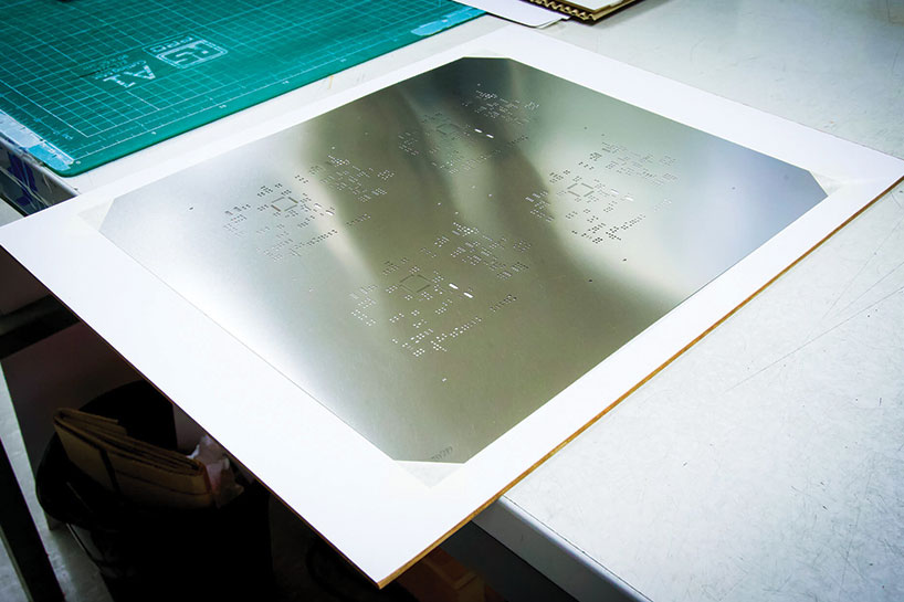
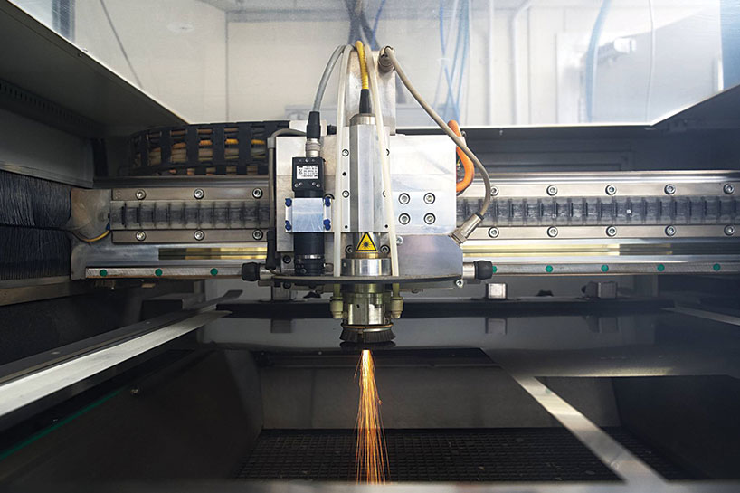
Solder stencils are stainless steel sheets used in the PCB assembly process. Typically laser-cut, they have become more popular in recent years thanks to the industry’s adoption of surface mount technology, and their creation is one of the many services we offer here at PCB Train.
In the blog below, we’ll explore solder stencils in more detail and explain just why they are so vital to modern PCB production.
What Are Solder Stencils?
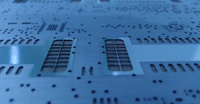
Stainless steel stencils help PCB technicians to deposit solder paste onto bare printed circuit boards more accurately. This is made possible by the existence of holes, or apertures, in the stencil that reflect the size and position of surface mount devices (SMDs) on printed circuit boards. The rise of SMDs has spearheaded PCB stencil popularity, with the manual application of solder now considered too clumsy or random to be effective.
Even though solder stencils can speed up PCB assembly, it should be noted that this does not lead to a decline in quality. In fact, using a solder stencil has been shown to reduce mistakes and failures at any point in the PCB’s lifespan, and will actually strengthen the connection between SMT pads and their components. It can also save considerable amounts of time and money.
Many PCB manufacturers, including ourselves, use solder stencils to apply solder paste to printed circuit boards. This ensures that all electronic components adhere to the boards without issue, whilst aiding long-term connectivity. The use of a high-performance solder paste will also help to minimise oxidation damage when the PCB is placed in a reflow oven.
How Do PCB Stencils Work?
Thanks to fiducial marks, which help to align the stencil on top of the PCB, the application of solder via stencils is a seamless process. Once the stencil is aligned, skilled technicians will use a squeegee blade to make sure the right amount of solder is pushed through each precision-cut aperture. The time this takes in comparison to traditional soldering is minimal and offers vastly improved rates of uniformity and connectivity.
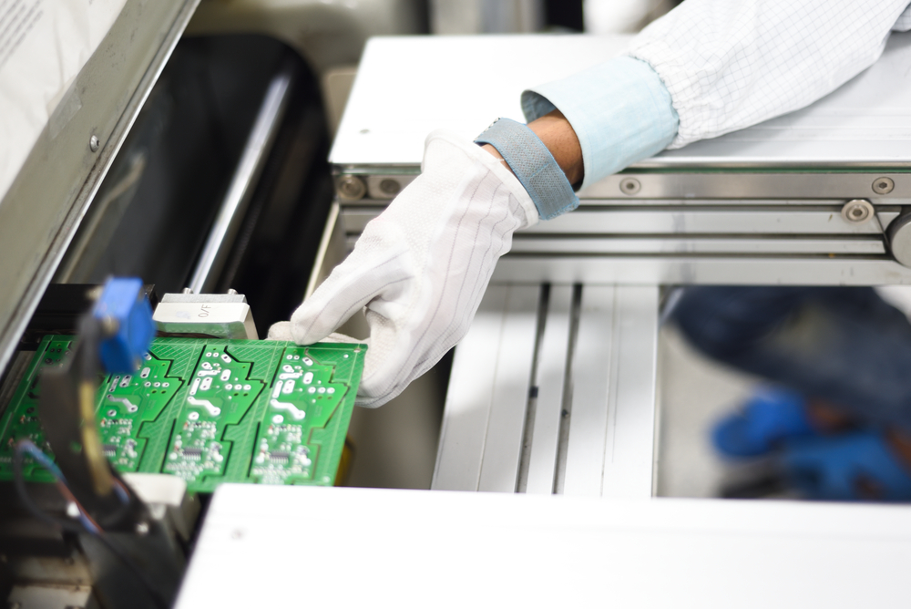
After the solder has been applied, surface mount devices will be added to your board via an automated process. The assembled PCB is then ready for wave or reflow soldering. These are processes in which the solder is melted, connecting the components to the board. Although wave soldering is recommended for designs that combine through-hole and surface mount technology, the best course of action for your PCB will be discussed with you by your chosen manufacturer before any work takes place.
Solder Stencils At PCB Train
Even though using solder stencils in PCB assembly may sound rather simple, there are plenty of potential pitfalls. That’s why it’s always important to consult a professional when you’re putting your design together. These people will be able to choose the correct thickness of steel stencil and create apertures of an appropriate size for your PCB.
PCB Train is proud to provide two different solder stencil services to ensure that you have everything you need to produce the highest quality printed circuit board. The first of these – Express – is best suited to those who are at the prototype stage or interested in a smaller production run, and as such, there are limitations on what we can provide. By contrast, our Full service has many more features, with a range of thicknesses, unlimited apertures and fiducial markers included as standard. This is recommended for stencils that are to be used in production solder pasting machines.
To find out what we advise for your PCB project, please get in touch with us today.
pcbtrain
Latest posts by pcbtrain (see all)
- Rapid PCB Prototyping with PCB Train Express - 5th July 2023
- 5 Good Reasons Why You Should Use PCB CAD Layout Design Services - 14th June 2023
- How To Become A PCB Designer - 1st November 2022


Leave a Reply