
What are printed circuit boards used for?
Today’s electronics wouldn’t be possible without the use of printed circuit boards in their manufacture and as such, they can be found everywhere. They have revolutionised the industry making it possible to produce electronics on a much larger scale, electrically connecting electronic components and allowing for smaller, compact circuits.

Printed Circuit Boards are made from a combination of copper sheets laminated onto a non-conductive/insulating substrate. The insulating surface material is etched as part of the manufacturing process to reveal the conductive metal which creating conductive paths through which electricity can travel through the components which are mounted to the board.
Examples of where they can be found:
- Computers
- TVs
- LED Systems
- Switches
- Cars
- Mobile Phones
- Industrial Equipment
- Medical Devices
- Security Equipment
- Military Equipment
- Aerospace Industry
Who invented printed circuit boards?
Paul Eisler an Austrian has been credited with inventing the printed circuit board in 1936 to operate a radio system. In 1948 the idea of a PCB was made public by the US Army, with the American electronics industry developing it rapidly in the 1950s, followed by Europe.
Are printed circuit boards toxic?
Whilst printed circuit boards themselves aren’t toxic, burning them and their components as part of a waste process can cause toxic substances to be released. For this reason, PCBs should always be properly disposed of or recycled.
The most common reason why PCBs are associated with being toxic to an uninformed person is due to their historic association to the abbreviation “PCB” which refers to the harmful chemical Polychlorinated Biphenyl, which is NOT a component of printed circuit boards.
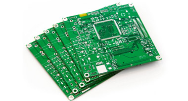
Why are printed circuit boards green?
It is the outer covering called the solder mask which is green rather than the circuit board entirely. Green is the most commonly used colour however really any colour such as blue or red could be used.
Reasons why green is the industry standard:
- Green causes less eye strain, helping to decrease any fatigue caused to technicians who need to inspect them
- Green is typically the cheapest colour to manufacture due to the popularity of naturally green epoxy coating
- The use of green was a regulation for PCB manufacture ordered by the US military as they found it the most effective in many of the tests they carried out. As many PCB manufacturers supplied the military it made sense to use the same colour of solder mask for their non-military customers which would cost them less.
Can printed circuit boards be recycled?
The small amounts of copper within a bare circuit board can be recycled however the epoxy coating is not recyclable. Many scrap metal merchants are prepared to purchase bulk amounts of PCBs to make recycling economical.
You can read more about recycling PCBs and the recycling process at the Newbury Group Here.
Can printed circuit boards be repaired?
Whether a PCB can be repaired depends upon the level and type of damage that it has been subject to. For example, if your circuit board has been melted or heat damaged this is more likely to be irreparable than if you’re experiencing a short circuit which perhaps requires cutting out.
Any repairs would of course also depend on the economics; determining whether you’re better investing time and money in repairing the existing board or manufacturing a new one to carry out the function, particularly if you have the original designs.
Get in touch with our team on +44 (0) 1635 40347 or via our online contact form to discuss your damaged circuit board and whether we’d be able to assist you with repairs.
How many types of PCB are there?
There are 6 main types of printed circuit boards, named after their number of layers and flexibility:
Layered:
- Single-sided PCBs – Basic circuit board with all components on one side comprising of a single conductive copper layer on the substrate and then the solder mask.
- Double-sided PCBs – Consist of copper and solder mask added on both sides of the substrate/board. This means that components can be mounted to both sides and circuits connected through holes drilled into the board.
- Multi-Layered PCBs – Consist of multiples of single and double-sided boards with insulation between each board to protect components. Multi-layer PCBs tend to make up more complex circuit systems such as those found in GPS, data storage and satellites.
Flexibility:
- Rigid PCBs- These boards cannot be twisted, bent or folded and can refer to single, double or multi-layered PCBs. Commonly used in computers where strength is required in a circuit.
- Flexible PCBs – These boards can be flexed and bent around corners meaning they are ideal for applications where space is key, such as in phones LCDs and cameras.
- Flexi-Rigid PCBs – Combine both flexible and rigid boards. Typically the flexible element of the board is used to interconnect rigid boards giving the best of both worlds.
Do you have questions about PCBs or the Manufacturing process here at PCB Train? Have a read of our FAQs or get in touch with our team here for your answers.
Philip King
Latest posts by Philip King (see all)
- How to Design an Enclosure for a Printed Circuit Board Assembly (PCBA) - 18th June 2026
- Understanding IPC Standards in PCB Fabrication and Assembly - 2nd June 2026
- SMD PCBs: What They Are And Where They Are Used - 7th October 2022


Leave a Reply