
The creation of a printed circuit board can be a lengthy process and will require input from many technical professionals. What starts out as a two-dimensional, computer-based roadmap will eventually be tasked with ensuring the smooth running of an electronic device. And it’s no small journey to get there.
To reach this intended goal, PCBs need to go through many intricate design phases overseen by experienced engineers. It is only then that they will be able to perform at the very highest level.
The Beginning: PCB Schematics
It is the role of a PCB designer to use computer-aided design (CAD) software to put together a blueprint of the different components that are to be featured in a PCB. Known as a PCB schematic, this initial design is a visual depiction of everything that needs to be included to make the circuit work. The schematic should also set out how the components will connect and function. It is by no means a final representation of what the PCB will look like when assembled.

Often designed with the help of advanced CAD software, PCB schematics are still sometimes hand-drawn with accompanying instructions. Many professionals prefer to use computer programmes to speed up the process and reduce errors.
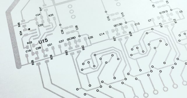
The Middle: Design Layout
When completed, the PCB’s blueprint, or schematic capture, plays an important role in the next stage of the design process: the layout. It is within this phase that the ideas mapped out in the schematic become something more tangible.
Certain CAD programmes allow designers to place components and copper traces onto a visual representation of a circuit board. The aim here is to create a circuit that performs its duties correctly and without issue. Things to consider at this stage include the proximity of certain components to each other, crossed traces and taking steps not to overcrowd the board. Devising an appropriate layout will also increase in difficulty if the aim is to create a PCB with multiple layers.
For those working with actual 3D models, the same considerations apply. It may just be more costly to make a mistake as physical materials are being used. Something else to remember is that the physical layout of the PCB may differ greatly from how it appears on the schematics. This is completely normal. You should see the layout stage as a testing phase and work hard to make sure all of the components interact without error. Be prepared to revise your setup if things don’t work out as expected.
The End: Design Finalised
Once changes have been made and you are satisfied with the results of your latest test phase, your PCB design should be good to go. If you don’t have the facilities to produce this on a mass scale, a completed PCB design can be shared with manufacturers such as PCB Train to help your product become a reality.
As the sister company of Newbury Electronics, we specialise in the fabrication and assembly of high-quality PCBs for numerous clients in a wide range of industries. Our extensive CAD services can guide you through each crucial step of PCB design, with our experts using their considerable knowledge to guarantee that your circuit board achieves its full potential.
To discover more, please email us at pcbtrain@newburyelectronics.co.uk or give us a call on +44 (0) 1635 40347 today.
pcbtrain
Latest posts by pcbtrain (see all)
- Rapid PCB Prototyping with PCB Train Express - 5th July 2023
- 5 Good Reasons Why You Should Use PCB CAD Layout Design Services - 14th June 2023
- How To Become A PCB Designer - 1st November 2022


Leave a Reply