
High-quality PCBs are important to the success of your electronic product, but where do you start when putting your own circuit board together? This is where PCB CAD layout design services can help!
Discover 5 good reasons why you should use a PCB CAD layout design service rather than opting to design a PCB circuit yourself.
1. Expert knowledge of suitable base materials
Choices have to be made to select the appropriate base material and copper thickness required. This will depend on the operational environment and the current load of the circuit. Inappropriate material selection can easily cause premature circuit failures in the field.
2. In-depth understanding of the trade-off between component density and PCB complexity
Choices have to be made regarding the number of copper layers that the CAD layout requires. This is influenced by the final target cost, circuit complexity, desired physical size, and EMC amongst other factors. Poor selection of these factors may cause circuit failure at the prototype stage, and necessitate complete redesign and substantial additional costs.
3. Anticipation of and resolution of potential thermal and EMC (electromagnetic compatibility) problems
Foreseeing these issues during the design process can ensure that they simply do not become a problem. However, failure to design in adequate solutions and precautions can require a complete redesign after prototype testing. This adds untold extra costs and delays to the project.
4. Design for manufacture
Extensive knowledge of manufacturing PCBs is essential to ensure that both a bare PCB can be made without fundamental design errors, and also that it can be efficiently populated by machine processes such as CNC pick and place, CNC de-paneling machines, and automated selective soldering machines, amongst others.
5. Design for safety
Care must be taken to ensure that the correct clearances between copper tracks are designed into the PCB CAD layout where high voltages are present. Tracks that are laid too close together may sustain arcing or voltage creep during service, resulting in catastrophic failure.
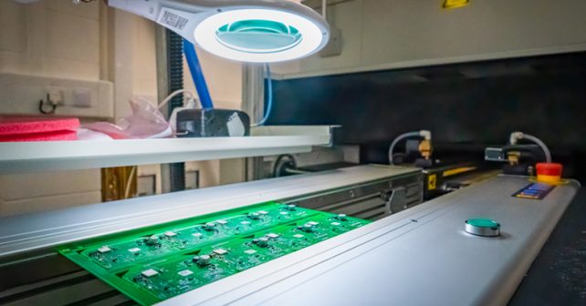
High-Quality PCB Manufacturers UK
PCB Train has over 65 years of experience in delivering reliable, high-performance printed circuit boards. Our team will always use the best materials to ensure that your PCB is fit for the job.
Get a quote online today or get in touch with our team to find out more about our services and how we can help you!
pcbtrain
Latest posts by pcbtrain (see all)
- Rapid PCB Prototyping with PCB Train Express - 5th July 2023
- 5 Good Reasons Why You Should Use PCB CAD Layout Design Services - 14th June 2023
- How To Become A PCB Designer - 1st November 2022


Leave a Reply