
What is CAD?
CAD, or Computer Aided Design is the process of using computer software to draw, design and develop a product or concept. CAD programs allow a person to create a visual representation of an object. It is extremely useful to a number of industries. This includes naval and aero engineering, architectural and product design industries now use CAD prolifically. This is also the case in printed circuit board design and production.
PCBs and CAD
CAD is used during the development process of creating a PCB. There are many different types of CAD software to choose from. Take a look at our useful links page for access to free software, such as Design Spark, KICAD and FreePCB. Though they basically do the same thing, every CAD program works slightly differently, so a designer will choose the one that suits them best.
Schematic capture
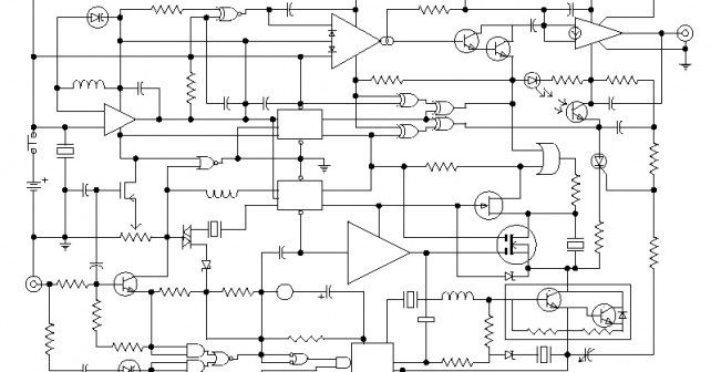
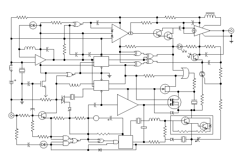
This design process begins with the CAD technician mapping the component positioning and connections that will be on the PCB. This is known as ‘schematic capture’ in PCB talk. The CAD schematic acts as a sort of blue print for the circuit that is being designed. It determines what components will be in the PCB and how they are joined. The electrical traces on a schematic are called ‘nets’. A designer can use an existing schematic design, or create their own. A designer will run simulations to test how well the schematic will operate as an actual circuit. This is one of the major benefits of CAD; when circuit designs were hand-drawn such faults would not be noticed until the circuit had actually been made.
Turning a schematic capture into a circuit
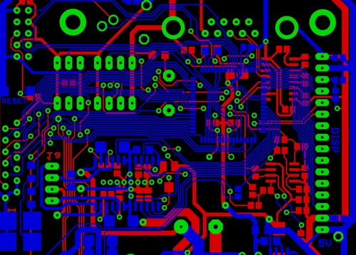
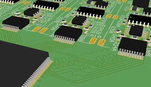
Once a schematic has been tested and approved the design must be transferred into an actual CAD drawing of the circuit board. The dimensions of the board are realised, along with the placement of the components and the copper trace connections. Often, programs will have a ‘switch to board’ (or similar) command on the CAD program. This allows you to place components onto your on screen board. The CAD designer places the components and labels them with their name and value. When designing the schematic the grid is not important, but it becomes crucial when editing the actual board. The movement tool is selected to move parts about (called different things in different CAD programs) and they can be rotated to fit onto your board. A designer will try not to overcrowd components or cross your copper traces, as this would cause the circuit to short.
The CAD circuit will become more complicated as you add multiple circuit board layers. A designer will usually route one layer horizontally and the next one vertically. Allowances should also be made for the physicality of components. Taller ones will have to be placed in certain areas, depending on the final destination of the circuit board. The components must have the complete information that they would require to be a part of the board. This includes any drilling information, the footprint for the board pads etc.
Routing
This is the stage in which the designer routes the copper connections between the components. The CAD software will route the connections in accordance with information from the schematic capture. Often, the CAD software will have a ‘route’ tool to assist with manual routing. However there are also programs that have auto routing software. As mentioned earlier, the crossing of traces must be avoided when routing. If traces need to be crossed, the designer will make it so they cross on opposing sides of the board. Traces can be transferred from one side of the board to another using ‘vias’: these are small drill-holes that are loaded with copper on an actual circuit. Once all the copper traces have been routed the CAD program will often have an option that checks for errors in the PCB design. Once all the errors are corrected the PCB design is complete and ready to be made into a real circuit.
pcbtrain
Latest posts by pcbtrain (see all)
- Rapid PCB Prototyping with PCB Train Express - 5th July 2023
- 5 Good Reasons Why You Should Use PCB CAD Layout Design Services - 14th June 2023
- How To Become A PCB Designer - 1st November 2022


Leave a Reply